
Scientists in Japan have developed a new process for the fabrication of crystalline tin monosulfide (SnS). By facilitating the growth of crystals measuring up to 24mm in diameter, the process could help overcome some of the challenges to squeezing higher efficiencies out of this cheap, abundant material.
New thin film materials have an important role to play in solar technology’s future. Though most have far to go before generating commercial interest, offering potential for integration in flexible or semi-transparent devices, as well as layers in a multi-junction ‘tandem’ device further into the future. And with concerns over material consumption in solar becoming ever more prominent, discovering alternatives to the sometimes rare, expensive and toxic used in today’s thin film PV technologies is another long-term goal.
Though known as a cheap, abundant material with promising characteristics for use in solar cells, tin monosulfide (SnS) has proved a challenging material to work with, and researchers have so far struggled to achieve conversion efficiencies better than 5% with this material, and interest from the research community has lagged behind that of kesterite, or copper-zinc-tin, solar cells.
The challenge, according to scientists at Japan’s Tohoku University, lies in producing n-type SnS, necessary to form a junction with the much easier to fabricate p-type equivalent. Given its theoretical potential for solar cell efficiency beyond 30%, as well as the fact that tin already boasts a sophisticated supply chain, and mature industrial to produce tin-based thin films already exist, overcoming this challenge is an attractive prospect for researchers.
Molten flux
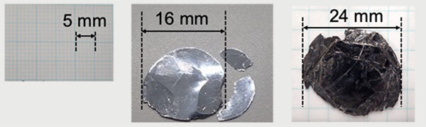
A group of scientists at Tohoku set about developing a process to grow SnS crystalline from a molten tin flux. The group found that adding halogen elements (in this case chlorine and bromine) to the flux led to the growth of much larger and thicker crystals – they measured a maximum of 16mm diameter and 0.7mm thickness for chlorine-doped SnS, and 24mm diameter, 1mm thickness with bromine.
The growth process is described in the paper Growth of Large Single Crystals of n-Type SnS from Halogen-Added SnS Flux, published in the journal Crystal Growth and Design. The group went on to measure the electrical characteristics of the thin film, observing encouraging electrical conductivity characteristics and confirming the material’s n-type conductivity.
“The large single crystals of n-type SnSn obtained in this work would enable the fabrication of p-n homojunction SnS solar cells via the deposition of p-type SnS thin films,” the paper concludes.
Lắp đặt điện mặt trời Khải Minh Tech
https://ift.tt/2X7bF6x
0906633505
info.khaiminhtech@gmail.com
80/39 Trần Quang Diệu, Phường 14, Quận 3
Lắp đặt điện mặt trời Khải Minh Tech
https://ift.tt/2ZH4TRU
Không có nhận xét nào:
Đăng nhận xét