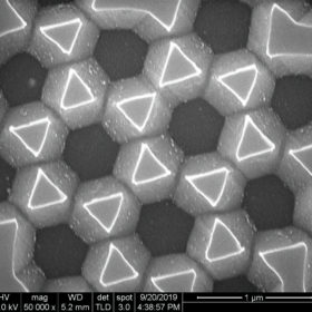
Scientists in South Korea combined two processes to etch a nanostructure of tiny pyramids onto the surface of a silicon wafer. As well as trapping more light and increasing the cell efficiency, the group claims that its nanostructure improves the mechanical flexibility of the cells. This could potentially allow for the use of much thinner silicon wafers than is currently possible in production.
Wafers used in cell production today are typically 180-200 microns thick. Going thinner than this is widely thought to bring about problems with the wafer being too fragile to withstand the stresses it is put through both during production and in the field. And since the cost of polysilicon has fallen continually in recent years, manufacturers lack a strong incentive to cut down on consumption.
Among researchers though, there is still plenty of interest in ‘ultrathin’ cells at thicknesses of 50 microns or less. As well as saving on polysilicon costs, these could lead to much lighter and more flexible cells suitable for applications beyond conventional PV modules. And scientists also theorize that working with ultrathin wafers could open doors to higher efficiency achievements.
Scientists led by the Korea Institute of Science and Technology (KIST) claim to have found a way to increase the mechanical flexibility of cells 50 microns thick, by etching a light-trapping nanostructure onto their surface.
Light trapping
Cells in production are typically etched with a pyramid-like structure, which ‘traps’ more light, preventing it from being reflected away from the cell. The group at KIST investigated ways to make this pyramid structure even smaller, and found that they could achieve results comparable to conventional processes, whilst significantly improving on the mechanical flexibility of the wafer.
The work is described in the paper Fabrication of quasi-hexagonal Si nanostructures and its application for flexible crystalline ultrathin Si solar cells, published in Solar Energy. The group used a combined process of nanosphere lithography and wet etching to fabricate cells with a quasi-hexagonal nanostructure on their surface. Cells etched with the nanostructure had a critical bending radius 46% lower than those with conventional pyramid etching, and showed efficiencies around 1% lower.
“The production of thin wafer-based solar cells is very challenging due to the fragility of the thin wafers. Thin wafers with surface cracks or textures are more prone to breakage because the surface microstructures act as stress concentration sites.” KIST senior researcher Inho Kim told pv magazine. “We do not have data about breakage yield of thin wafers in production. But we can say the breakage yield of the thin wafers textured with the nanostructures would be greatly reduced, compared with the conventionally textured (micro-pyramids) wafers.”
With further optimizations to its process, the group expects that its approach to nanostructuring could also yield better results in terms of light trapping and cell performance, on top of the demonstrated benefits to mechanical flexibility.
Lắp đặt điện mặt trời Khải Minh Tech
https://ift.tt/2X7bF6x
0906633505
info.khaiminhtech@gmail.com
80/39 Trần Quang Diệu, Phường 14, Quận 3
Lắp đặt điện mặt trời Khải Minh Tech
https://ift.tt/2ZH4TRU
Không có nhận xét nào:
Đăng nhận xét