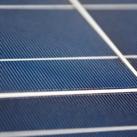
Researchers at the Massachusetts Institute of Technology, working with financial modeling teams at NREL, have projected the electrical losses and financial gains of thinning solar cells from the current 160 micrometers to 50 micrometers.
From pv magazine USA.
Solar module innovation is alive and well.
We’ve seen an increase in efficiency of almost 50% from an industry standard 15%, to Longi recently setting a mono PERC record at 22.38%. Just last week, Trina took the “large wafer” concept from the lab to manufacturing line in less than a year. And heterojunction solar modules seek to redefine what is possible.
Researchers at the Massachusetts Institute of Technology and the U.S. Department of Energy’s National Renewable Energy Laboratory have published a paper describing the potential technical and financial outcomes of pushing the solar cell manufacturing industry to thin its solar wafers from today’s industry standard of 160 micrometers (μm) to 50 μm. The paper, Revisiting thin silicon for photovoltaics: a technoeconomic perspective, also gives guidance on the various technologies that’d need to advance to enable this reality.

The first step the researchers took was revisiting an old idea — how thin is too thin when it comes to cutting solar ingots into solar wafers? Generally speaking, thinning wafers reduces their ability to capture available photons, especially those photons in the near-infrared spectral range. We thought we’d found a sweet spot at 160 μm thick, however these scientists simulated the thicknesses in the above images across multiple modern and future solar wafer types and came to a conclusion that we can do better.
The researchers note when considering the case of “1 ms bulk lifetime,” the efficiency of 50 μm versus 160 μm thicknesses are 101%, 98%, 97%, and 97% from left to right in the above image — using almost 69% less silicon.
In the above images, AL-BSF represent historically standard aluminum back screen wafers, PERC represents the current product’s we’re buying today, while advanced PERC represents products that we can buy at the cutting edge – like REC Group’s Alpha Product, or Trina and Jinko’s TOPcon products. “Adv HE-Tech” represents future heterojunction products, with advanced efficiencies and qualities designed to take advantage of “thin wafers.”

To give you a broader feel for the difference between the current and our cutting-edge future, the above table compares a standard mono PERC wafer at 160 μm versus the advanced heterojunction 50 μm product. Note that kerf loss (wasted silicon ingot between each wafer cut away) goes from 95 μm to 28 μm – which essentially means that almost two entire advanced solar wafers are lost making one modern wafer today.
More notably though, notice how module prices fall from 32¢/W to 20¢/W — a 37.5% fall. Note that it also drops the non-subsidized cost of electricity from these modules, on a power plant level, by 23% – a not trivial number at all. One important thing to note on that 32¢/W price for modern modules – the number is from 2018. We’re currently reaching 24-20¢/W for standard mono PERC modules that are greater than 19% efficiency.
This author speculates that we could adjust the value to consider modern mono PERC at the above mentioned 20 to 24¢/W – and adjust the advanced heterojunction 50 μm product down to a range of 15 to 12.5¢/W for modules.
The report authors looked across the entirety of the solar module manufacturing process and found multiple areas in the process where money could be saved. Looking at 2010 to 2018, the total capex for module production from raw silicon to module declined by 75% from $1.52 to $0.39/watt per year. The advanced heterojunction 50 μm wafers could potentially reduce manufacturing capex by 48% further.

A relationship was found where with every 10 μm thickness reduction, manufacturing capex declines roughly by 1.3¢/W/year, and module cost declines roughly by 0.6¢/W/year. The authors found that thin silicon, regardless of whether using existing, cutting edge, or developing cells can reduce cost of electricity by more than 5% relative to 160 μm wafers. To put it in perspective, the industry has transitioned to PERC to harness the 3% reduction in LCOE.
To gain the greatest benefits put forth in this paper, those of the advanced heterojunction solar cell, new solutions must be found in multiple areas as noted in the below chart. For instance, we need to learn how to cut thinner wafers. The current cut is a 255 μm cut, with 95 μm of that being wasted, whereas cutting edge described here is 78 μm — and 70% lesser silicon. Imagine how the silicon ingot manufacturers – feeling massive pricing pressures – might feel if their product suddenly generated three times more than its current value.

Lắp đặt điện mặt trời Khải Minh Tech
https://ift.tt/2X7bF6x
0906633505
info.khaiminhtech@gmail.com
80/39 Trần Quang Diệu, Phường 14, Quận 3
Lắp đặt điện mặt trời Khải Minh Tech
https://ift.tt/2ZH4TRU
Không có nhận xét nào:
Đăng nhận xét